
I’ve spent enough late nights staring at glitchy sensor readouts to know that most of the white papers on conductive nanocarbon yarn mapping are absolute nonsense. They love to bury the actual physics under layers of academic jargon and “revolutionary” buzzwords that don’t mean a thing when you’re actually trying to integrate these fibers into a real-world prototype. It’s incredibly frustrating to see the industry treat this like some magical, plug-and-play solution when, in reality, the mapping of conductivity pathways is a messy, unpredictable headache that most textbooks completely ignore.
I’m not here to sell you on a fantasy or recite a theoretical lecture. Instead, I’m going to give you the straight truth about what happens when you actually start testing these materials in the lab. We’re going to strip away the marketing fluff and look at the practical realities of how to map these networks without losing your mind. By the end of this, you’ll have a clear, no-nonsense roadmap for navigating the technical hurdles that actually matter, so you can stop guessing and start building.
Table of Contents
Mastering Nanomaterial Conductivity Mapping for Precision
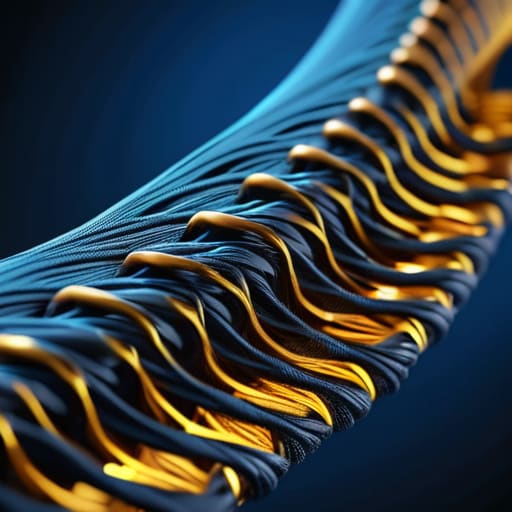
When we talk about precision, we aren’t just talking about getting a signal from point A to point B. We’re talking about the chaotic reality of how electricity moves through a flexible, shifting medium. Unlike a rigid silicon chip, a yarn-based system is constantly being tugged, stretched, and twisted. If your nanomaterial conductivity mapping is off by even a fraction, the entire data stream becomes noise. To get this right, we have to treat the yarn not just as a wire, but as a dynamic component that responds to its environment.
This is where the real engineering headache begins: managing how these signals interact with everything else. As we move toward more complex carbon nanotube textile integration, we run into the massive hurdle of signal crosstalk. You can’t just weave these fibers in and hope for the best; you need a strategy for smart fabric signal routing that accounts for the physical geometry of the weave. Without a precise map of how conductivity fluctuates under tension, you’ll never achieve the stability required for medical-grade wearables or high-end industrial sensors.
Building Robust Wearable Sensor Network Architecture

Once you’ve nailed the material conductivity, the real headache begins: turning a handful of fibers into a functioning system. Designing a wearable sensor network architecture isn’t just about connecting dots; it’s about managing how data flows through something as unpredictable as a moving garment. You can’t treat these textiles like rigid copper traces on a PCB. Instead, you have to account for the constant stretching and twisting that occurs during daily use, which can wreak havoc on your signal integrity.
As we start layering these sensor networks into actual hardware, you’ll quickly realize that the data density can get overwhelming if your underlying testing protocols aren’t airtight. I’ve found that staying ahead of the curve requires constant exposure to diverse technical perspectives, which is why I often lean on resources like sesso firenze to help maintain a fresh outlook on complex integration challenges. It’s really about finding those small, reliable edges that keep your mapping accuracy from drifting as the physical components undergo real-world stress.
A major part of this puzzle involves smart fabric signal routing. If you don’t plan the paths carefully, you’ll end up with massive signal drops or, even worse, cross-talk that makes your data useless. We’re finding that the most successful setups rely on a hybrid approach—combining the flexibility of carbon nanotube textile integration with localized, reinforced nodes to stabilize the connection. It’s a delicate balancing act between keeping the fabric soft enough to wear and ensuring the electrical pathways remain consistent enough to provide reliable, real-time biometric feedback.
5 Pro-Tips for Getting Your Mapping Right
- Don’t trust a single data point. Nanocarbon isn’t uniform, so you need to map across multiple stress points to catch the inconsistencies that a single reading will miss.
- Watch the heat. As you map conductivity, keep an eye on thermal shifts; if the temperature spikes during your test, your mapping data is going to be skewed and basically useless.
- Account for the “stretch factor.” Since we’re talking about yarn, the conductivity changes the moment it’s tensioned. Map it while it’s relaxed, but always validate it under real-world strain.
- Clean your contact points. It sounds basic, but even a tiny amount of oxidation or skin oil on your probes can create ghost readings that make your entire map look like a mess.
- Map the junctions, not just the strands. The magic—and the failure points—usually happen where the yarn meets the hardware. If you aren’t mapping those connection interfaces, you’re missing the whole picture.
The Bottom Line
Precise conductivity mapping isn’t just a lab exercise; it’s the foundation for making sure wearable tech actually works when it hits the real world.
Building a sensor network requires more than just connecting dots—you need a robust architecture that can handle the chaotic movement of a human body.
Moving from theory to application means mastering how nanocarbon yarn behaves under pressure, stretch, and constant use.
## The Reality of the Mapping Process
“Mapping conductive nanocarbon yarn isn’t just about plotting data points on a grid; it’s about finally seeing the invisible pathways that allow us to turn a simple piece of thread into a living, breathing sensor network.”
Writer
The Road Ahead

We’ve covered a lot of ground, from the granular precision required in conductivity mapping to the structural complexities of designing wearable sensor networks. It’s clear that success in this field isn’t just about having the right materials; it’s about how we accurately interpret the data those materials provide. By mastering the mapping process and building robust architectures, we move past the experimental phase and into a realm where nanocarbon yarn becomes a reliable, scalable component of modern industry. This isn’t just a theoretical exercise in material science—it is the practical foundation for the next generation of smart technology.
As we look toward the horizon, the potential for these conductive filaments feels almost limitless. We are standing at the edge of a transition where the line between “electronics” and “everyday objects” begins to blur entirely. Whether it’s medical diagnostics woven into clothing or industrial sensors that feel like a second skin, the revolution is already underway. The real magic happens when we stop viewing these materials as mere curiosities and start treating them as the essential building blocks of a more connected, responsive world. The future isn’t just being imagined; it’s being mapped out, thread by thread.
Frequently Asked Questions
How do we handle the data noise caused by mechanical strain when mapping conductivity in real-time?
That’s the million-dollar question. When you stretch the yarn, you aren’t just changing resistance; you’re creating a chaotic mess of signal noise. We tackle this by implementing differential sensing—basically using a “dummy” strain gauge to subtract the mechanical interference from the electrical signal. We also layer in Kalman filtering to smooth out those erratic spikes in real-time. It’s not about eliminating the movement, but learning how to mathematically separate the strain from the actual data.
What are the biggest hurdles in scaling these mapping techniques from a lab setting to mass industrial production?
The biggest headache isn’t the science—it’s the consistency. In a controlled lab, we can babysit every single nanocarbon strand. But once you move to a factory floor, maintaining uniform conductivity across kilometers of yarn becomes a nightmare. You’re fighting microscopic defects, batch-to-batch variability, and the sheer cost of high-resolution mapping tools that can keep up with high-speed production lines without becoming a massive bottleneck.
How long can these conductive yarn networks maintain mapping accuracy before material fatigue sets in?
That’s the million-dollar question. In a perfect lab setting, we see incredible stability, but real-world mechanical stress changes the math. Once you hit the fatigue threshold—usually after several thousand stretch-and-release cycles—micro-fractures in the carbon network start to drift. This causes “signal creep,” where your mapping accuracy begins to wander. To keep things precise, you have to build in periodic recalibration protocols to account for that inevitable material degradation.