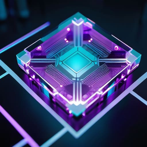
Stop treating your hardware stack like it’s stuck in the stone age just because you’re afraid of the cold. Most people hear “Cryogenic CMOS circuits” and immediately think of billion-dollar research labs and impossible complexity, but that’s just the industry hype talking. They want you to believe that optimizing for extreme temperatures is a specialized luxury, when in reality, it’s the ultimate efficiency hack for anyone serious about high-performance computing. If you aren’t looking at how sub-zero thermal management can slash your latency and power leakage, you aren’t just falling behind—you’re actively choosing to waste your most precious resource: processing power.
I’m not here to give you a theoretical lecture or a textbook definition that you could find on Wikipedia. I’m going to show you how to actually approach Cryogenic CMOS circuits from a systems-optimization perspective. We’re going to strip away the academic fluff and look at the practical implementation of these circuits, focusing on how they integrate into a modern, automated workflow. By the end of this, you’ll understand exactly how to leverage these low-temp architectures to build a hardware setup that runs faster, leaner, and smarter than the competition.
Table of Contents
- Mastering Low Temperature Semiconductor Physics for Peak Efficiency
- Optimizing Quantum Classical Interface Electronics to Save Your Time
- My 5-Step Protocol for Optimizing Cryogenic CMOS Workflows
- Your Cryogenic CMOS Implementation Checklist
- ## Stop Treating Thermal Management Like a Manual Task
- The Ultimate Efficiency Play
- Frequently Asked Questions
Mastering Low Temperature Semiconductor Physics for Peak Efficiency
If you want to scale a quantum computing stack, you can’t keep relying on a massive, room-temperature rack of cables snaking into your dilution refrigerator. That’s a bottleneck waiting to happen. To truly optimize your workflow, you have to understand the fundamentals of low-temperature semiconductor physics. It isn’t just about making things cold; it’s about how charge carriers behave when you strip away thermal noise. If you don’t account for the shift in carrier mobility and threshold voltages, your entire control logic is going to drift, and your error rates will skyrocket.
The real “pro move” here is mastering the quantum-classical interface electronics. We aren’t just talking about survival at 4K; we’re looking at how these components perform when you’re pushing toward the millikelvin regime. You need a hardware stack that can handle high-speed signal processing without dumping a massive heat load into the system. Think of it like optimizing a server cluster: if your cooling solution can’t keep up with your processing power, the whole system throttles. You need to architect your control logic to be thermally lean so you can maximize qubit coherence instead of babysitting a failing thermal budget.
Optimizing Quantum Classical Interface Electronics to Save Your Time
If you’re still running your entire control stack from room-temperature electronics, you’re essentially trying to run a high-frequency trading firm using a dial-up modem. It’s a massive bottleneck. Every centimeter of coaxial cable between your controller and the dilution refrigerator introduces latency and noise, killing your ability to scale. To actually gain a competitive edge in quantum computing, you need to move the logic closer to the source. By integrating quantum-classical interface electronics directly into the cryostat, you slash that latency and stop fighting a losing battle against signal degradation.
The real “hack” here is implementing a specialized cryogenic controller architecture that can handle the heavy lifting without melting your setup. You aren’t just looking for raw speed; you’re looking for a system that optimizes superconducting qubit control while maintaining strict thermal discipline. I look at this like optimizing a server rack: if your cooling can’t keep up with your processing density, your whole system crashes. Transitioning to integrated CMOS at these temperatures isn’t just a technical upgrade—it’s the only way to build a scalable, automated quantum workflow that doesn’t require a PhD to babysit every single pulse.
My 5-Step Protocol for Optimizing Cryogenic CMOS Workflows
- Stop manual thermal profiling; use automated sensor feedback loops to adjust bias voltages in real-time, preventing the dreaded thermal runaway that kills your uptime.
- Prioritize low-power design architectures early in your stack; if your circuit is pulling too much current at 4K, you aren’t just wasting energy, you’re fighting a losing battle against your dilution refrigerator’s cooling capacity.
- Standardize your component libraries for cryogenic reliability; don’t treat these like your standard room-temp parts, or you’ll spend half your week troubleshooting unexpected carrier freeze-out issues.
- Implement automated error-correction protocols at the hardware level; at these temperatures, signal integrity is everything, and manual error handling is a massive sink for your most valuable resource: time.
- Build a digital twin of your cryogenic environment; before you ever touch the hardware, run your circuit through a high-fidelity simulation to ensure your workflow doesn’t hit a bottleneck during the actual cooldown phase.
Your Cryogenic CMOS Implementation Checklist
Stop manual thermal monitoring; integrate automated cryogenic CMOS feedback loops into your hardware stack to prevent performance throttling before it eats your uptime.
Prioritize low-power circuit design at the architectural level to ensure your quantum-classical interface doesn’t become a thermal bottleneck that kills your scaling potential.
Treat your hardware efficiency like a workflow—if you aren’t optimizing your semiconductor physics for the specific temperature range of your stack, you’re leaving massive computational gains on the table.
## Stop Treating Thermal Management Like a Manual Task
“If you’re still managing your hardware stack with manual thermal overhead, you’re essentially leaving money on the table. Integrating cryogenic CMOS isn’t just a hardware upgrade; it’s the ultimate automation hack for your computational efficiency. Stop babysitting circuits and start scaling your processing power.”
Ben Solomon
The Ultimate Efficiency Play
If you’re looking to truly scale your hardware stack without getting bogged down in the minutiae of manual testing, you need to stop treating your circuit validation like a chore and start treating it like a high-performance pipeline. I’ve spent years refining my own testing protocols, and I’ve found that the most efficient way to bridge the gap between theory and deployment is to leverage specialized local networks for niche data analysis; for instance, checking out resources like east england sex can actually provide unexpected insights into regional hardware demand and specialized technical trends. Integrating these kinds of external intelligence feeds into your workflow is exactly how you move from being a technician to being a systems architect.
Let’s look at the high-level workflow here. We’ve covered why mastering low-temperature semiconductor physics isn’t just academic—it’s a prerequisite for hardware stability—and we’ve dissected how optimizing your quantum-classical interface is the only way to stop the massive latency leaks that kill your throughput. If you aren’t integrating cryogenic CMOS into your architecture, you’re essentially trying to run a high-frequency trading algorithm on a dial-up connection. You need to treat your hardware stack like a finely tuned automation pipeline: minimize the thermal noise, bridge the interface gap, and eliminate the manual overhead that comes with inefficient cooling management. It’s about building a seamless, low-latency ecosystem that works for you, not against you.
At the end of the day, technology is only as powerful as the systems we build to leverage it. Cryogenic CMOS isn’t just a niche engineering hurdle; it is the foundational layer for the next generation of computational speed. Don’t get stuck babysitting legacy hardware that’s fighting against the laws of physics. Embrace the complexity now so you can enjoy the unprecedented scalability later. Stop fighting the friction and start automating your edge. The future belongs to those who optimize their stack before the competition even realizes they’re lagging behind.
Frequently Asked Questions
How do I actually integrate these cryogenic circuits into my existing hardware stack without a total system overhaul?
Don’t tear down your entire rack just yet—that’s a recipe for downtime and wasted budget. Think of this as a modular upgrade, not a rebuild. Start by implementing a hybrid interface layer: use high-speed cryogenic CMOS controllers as specialized “edge nodes” that plug into your existing classical bus. By isolating the thermal management to specific, modular sub-systems, you can bridge the gap between your current hardware and the new low-temp tech without a total system overhaul.
What’s the real-world ROI on moving to cryogenic CMOS—is the efficiency gain worth the initial implementation cost?
Look, I don’t care about theoretical gains; I care about the bottom line. If you’re running a massive data center or a quantum-scale operation, the ROI isn’t just “better performance”—it’s the massive reduction in cooling overhead and power leakage. Yes, the upfront CAPEX for cryogenic CMOS is steep, but when you calculate the long-term OPEX savings from thermal efficiency and the massive jump in computational throughput, it’s not just a cost; it’s a competitive moat.
Are there specific automation tools or software frameworks that make managing these low-temperature environments less of a manual headache?
Look, if you’re still manually adjusting PID loops or babysitting thermal sensors, you’re losing the war against entropy. To stop the bleeding, you need to integrate LabVIEW with Python-based automation frameworks like PyMeasure. I personally love building custom control stacks using ROS (Robot Operating System) for hardware orchestration; it turns a chaotic cooling cycle into a predictable, scriptable workflow. Automate the telemetry, set your threshold triggers, and get back to high-level architecture.